|
|
|
 www.design-reuse-china.com
 |
|

eSilicon revolutionizes machine learning ASIC platform (MLAP) market
neuASIC 7nm platform breaks down the barriers for machine learning ASIC design
SANTA CLARA, Calif. — June 5, 2018 — eSilicon, an independent provider of FinFET-class ASICs, custom IP, and advanced 2.5D packaging solutions, announced today at the Machine Learning and AI Developer’s Conference a fundamentally new approach to building application-specific integrated circuits (ASICs) for artificial intelligence (AI)/neural network applications called the neuASIC platform.
Up to now, hardware accelerators for machine learning have been built primarily with GPUs and FPGAs. The machine learning ASIC platform (MLAP) segment of the market has been under-served due to the dynamic nature of AI/machine learning algorithms. These algorithms typically experience a high degree of change as they are adapted to the end application, making it problematic to use a static, full-custom ASIC platform. It is well-known that an ASIC will deliver the best power, performance and lowest total cost of ownership but these benefits were out of reach for most due to frequent algorithm changes.
Drawing upon its work over the past three years on the design of AI/2.5D systems and recently announced production qualification for a deep learning ASIC, eSilicon has fundamentally changed the MLAP market segment with the neuASIC platform.
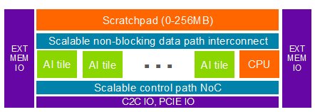
Through customized, targeted IP offered in 7nm FinFET technology and a modular design methodology, the neuASIC platform removes the restrictions imposed by changing AI algorithms. The platform includes a library of AI-targeted functions that can be quickly combined and configured to create custom AI algorithm accelerators. With the use of a Design Profiler and AI Engine Explorer, eSilicon-developed and third-party IP can be configured as AI “tiles” via an ASIC Chassis Builder, allowing early power, performance and area (PPA) analysis of various candidate architectures. The neuASIC platform also uses a sophisticated knowledge base to ensure optimal PPA.
The elements of neuASIC IP library include functions that are found in most AI designs, resulting in a core architecture that is both optimized and durable with respect to AI algorithm changes. Specific algorithm modifications can be accommodated through a combination of minor chip revisions that integrate appropriate AI “tiles” or modifications of the 2.5D package to integrate appropriate memory components.
eSilicon-developed AI-targeted “tiles” include subsystems such as: multiply-accumulate (MAC), convolution and transpose memory, among others. The physical interface to the HBM memory stack (or PHY) is also part of the library. Approximately 100 engineers at eSilicon are working on the design and silicon hardening of this AI IP.
A typical AI design requires access to large amounts of memory. This is usually accomplished with a combination of customized memory structures on the AI chip itself and off-chip access to dense 3D memory stacks called high-bandwidth memory (HBM). Access to these HBM stacks is accomplished through a technology called 2.5D integration. This technology employs a silicon substrate to tightly integrate the chip with HBM memory in a sophisticated multi-chip package. The current standard for this interface is HBM2. The development of customized on-chip memory and 2.5D integration represent eSilicon core competencies that are required for a successful AI design.
eSilicon built the industry’s first AI ASIC. The company is currently engaged with several tier one system providers and high-profile startups to deploy the neuASIC platform and its associated IP. Initial applications will focus on the data center and information optimization, human/machine interaction and autonomous vehicles.
“We see a vast array of possibilities for acceleration of AI algorithms,” said Patrick Soheili, vice president of business and corporate development at eSilicon. “ASICs provide a clear power and performance advantage. Thanks to our neuASIC platform, the MLAP segment of the market can now expand to serve a wide range of applications.”

neuASIC platform architecture
About eSilicon
eSilicon is an independent provider of complex FinFET-class ASICs, custom IP and advanced 2.5D packaging solutions. Our ASIC+IP synergies include complete 2.5D/HBM2 and TCAM platforms for FinFET technology at 14/16/7nm as well as SerDes, specialized memory compilers and I/O libraries. Supported by patented knowledge base and optimization technology, eSilicon delivers a transparent, collaborative, flexible customer experience to serve the high-bandwidth networking, high-performance computing, artificial intelligence (AI) and 5G infrastructure markets. www.esilicon.com


 Back
Back