|
|
|
 www.design-reuse-china.com
 |
|

Gowin Semiconductor Corp. announces LittleBee Family GW1NS Series GW1NS-2K FPGA SoC Device Engineering Samples and Development Board Available
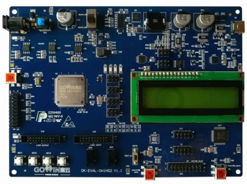
Guangzhou, CHINA -- July 24, 2018 – GOWIN Semiconductor Corp., the leading programmable logic devices provider in China, today announces Gowin first FPGA SoC devices LittleBee™ family GW1NS series, GW1NS-2, engineering samples and development board available now. The availability of GW1NS is the prologue of Gowin strategy on artificial intelligence (AI) and the emerging edge computing market.

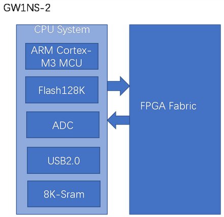
GW1NS-2 FPGA SoC device inherits the innovation of LittleBee™ family with embedded ARM Cortex-M3 hardcore processor and integrated USB2.0 PHY, user flash, SRAM read/write controller and ADC convertor, providing customers all-in-one embedded solution with programable logic features in one chip. With Gowin integrated development environment, engineers can develop their hardware and software in a single platform, which is another innovation of FPGA design platform and reduces engineering design cycle.
As the first Gowin FPGA SoC device, GW1NS-2 adopts ARM Cortex-M3 as embedded hardcore processor to utilize system control function with minimum internal memory. The integrated flexible and high performance FPGA logic elements provide high computational power for engineers to implement various efficiency control peripherals and exceptional system interrupts. As a member of LittleBee™ family, GW1NS-2 provides customers all leading features of the family like high performance logic, low power consumption, high IO to logic ratio, instant-on, non-volatile, high security, abundant package option, high design flexibility and low cost features.
GW1NS-2 FPGA SoC devices offer seamless connection between programmable logic devices and embedded processor, compatible with wide range of peripheral devices standard and reduce system cost significantly. GW1NS-2 is designed for various applications of industrial control, communication infrastructure, Internet-of-things, servo control, smart home, security encryption and consumer electronics.

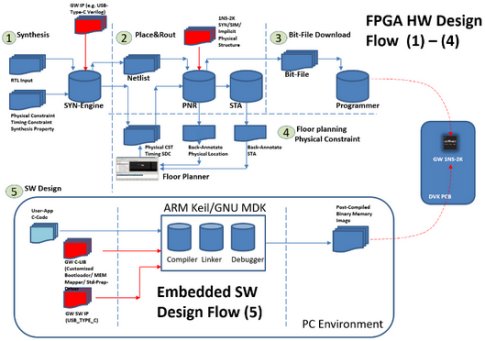
As shown in Figure1, the application development of GW1NS-2 FPGA SoC integrates hardware and software design flow, i.e., FPGA hardware logic design flow and embedded processor software design flow. The primary objective of FPGA SoC design is to configure the FPGA logic elements to be various physical peripherals of the embedded processor (CPU). After completing the architecture and hardware design with the FPGA logic, engineers can do embedded processor software programming to configure these peripherals. Gowin provides GW1NS-2 FPGA SoC devices and driver library, combining the software design tools (Compiler, Linker, Debugger) in an integrated development environment to support GW1N2-S FPGA SoC embedded processing programming; and also support ARM-MDK and GNU software design tools.
Gowin Semiconductor provides customers the new generation FPGA development environment supporting GW1NS series FPGA SoC device, which addressed the market needs and fully proprietary by Gowin Semiconductor Corp. The new development environment can perform FPGA synthesis, place and route, bitstream file generation and download in an one-stop integrated environment.
“GW1NS is a true miniaturized FPGA-SoC system in one chip,” said by Mr. Jim Gao, Senior Manager of IP core R&D department, Gowin Semiconductor Corp, “GW1NS leverages the advantages of FPGA programmable features to enable customers to design the interfaces and peripherals they needs in different applications scenarios with the integrated 1.7K LUTs low power FPGA logics, and configure these peripherals with the embedded CPU. The device directly integrates the data processing function of CPU with low density FPGA into one FPGA SoC system; such integration opens a new frontier of FPGA applications and systemization.
“GW1NS-2 is the first devices in the FPGA industry to integrate Cortex-M3 MCU and 1.7K LUTs logic in a single FPGA SoC”, said by Mr. TP Wang, Vice President of Engineering, Gowin Semiconductor Corp, “Gowin Semiconductor innovatively introduces low-density, non-volatile, embedded flash memory FPGA devices into wide range of market such as consumer, industrial control, IoT, security and get tremendous success in the market. GW1NS-2 FPGA SoC device fully utilizes the complementary features of MCU and FPGA, together with flexible peripherals of USB PHY and ADC, which widely extends the FPGA markets and applications. The availability of GW1NS-2 is also the prologue of Gowin strategy on AI and the emerging edge computing market. GW1NS series is the ideal embedded processor solution with programmability to address the applications like pattern and voice recognition in AI and edge computing end points”

Gowin Semiconductor always focus on product advantages accumulation, innovation and differentiation”, said by Stanley Tse, Reginal Sales Director of Gowin Semiconductor Corp, “The official launches of GW1NS-2 is our first trial on SoC market with our proven success LittleBee™ FPGA family + ARM hardware architecture. With this based architecture, we integrate high speed MIPI DPHY, ADC and other applications modules; together with our advantages on small package and low cost. We are very confident on market acceptance of GW1NS-2 and create another tremendous success of LittleBee™ family in broad range of applications, e.g., video interface, smart connected devices, portable consumer and ioT, AI and edge computing end points.
About GOWIN Semiconductor Corp.
Founded in 2014, GOWIN Semiconductor Corp., with headquarter and major R&D in China, our vision is to accelerate worldwide customers innovation by our programmable solution. We focus on optimizing our products and removing barriers for customers to use programmable logics devices. Our commitment to technology and quality enables customers to reduce total cost of ownership by using FPGA on their production boards. Our offering includes board portfolio of programmable logic devices, design software, intellectual property (IP) cores, reference designs and development kits. And we serves customers in consumer, industrial, communication, medical and automotive markets worldwide.
For more information about GOWIN, please visit www.gowinsemi.com


 Back
Back